AMAG nanometro
W CMP on AMAG7 Hardmask LineSpace
W CMP on AMAG7 Hardmask LineSpace
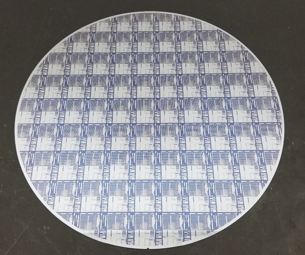
AMAG has developed Cu/W (copper/tungsten) CMP (chemical mechanical polishing) variants of AMAG7 at NYCreates. These variants are new standard AMAG7 wafer types, available for orders.
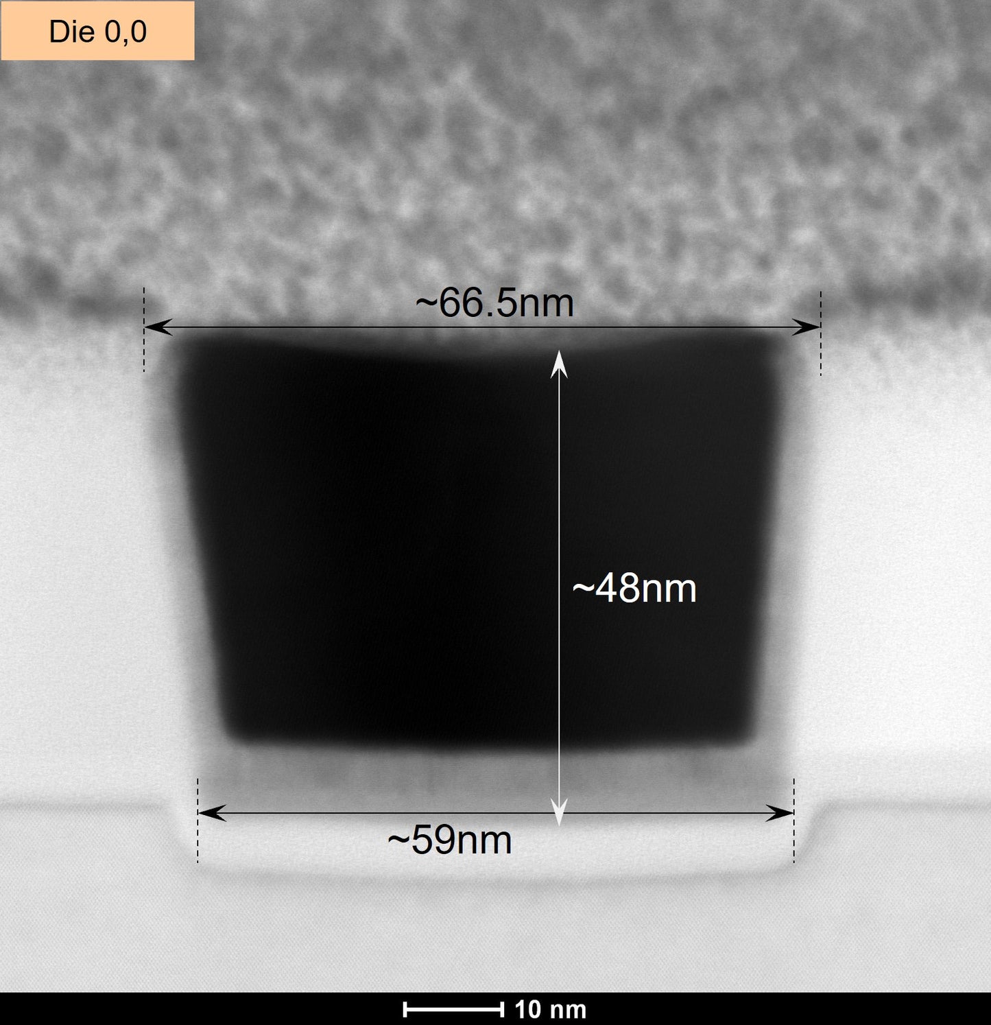
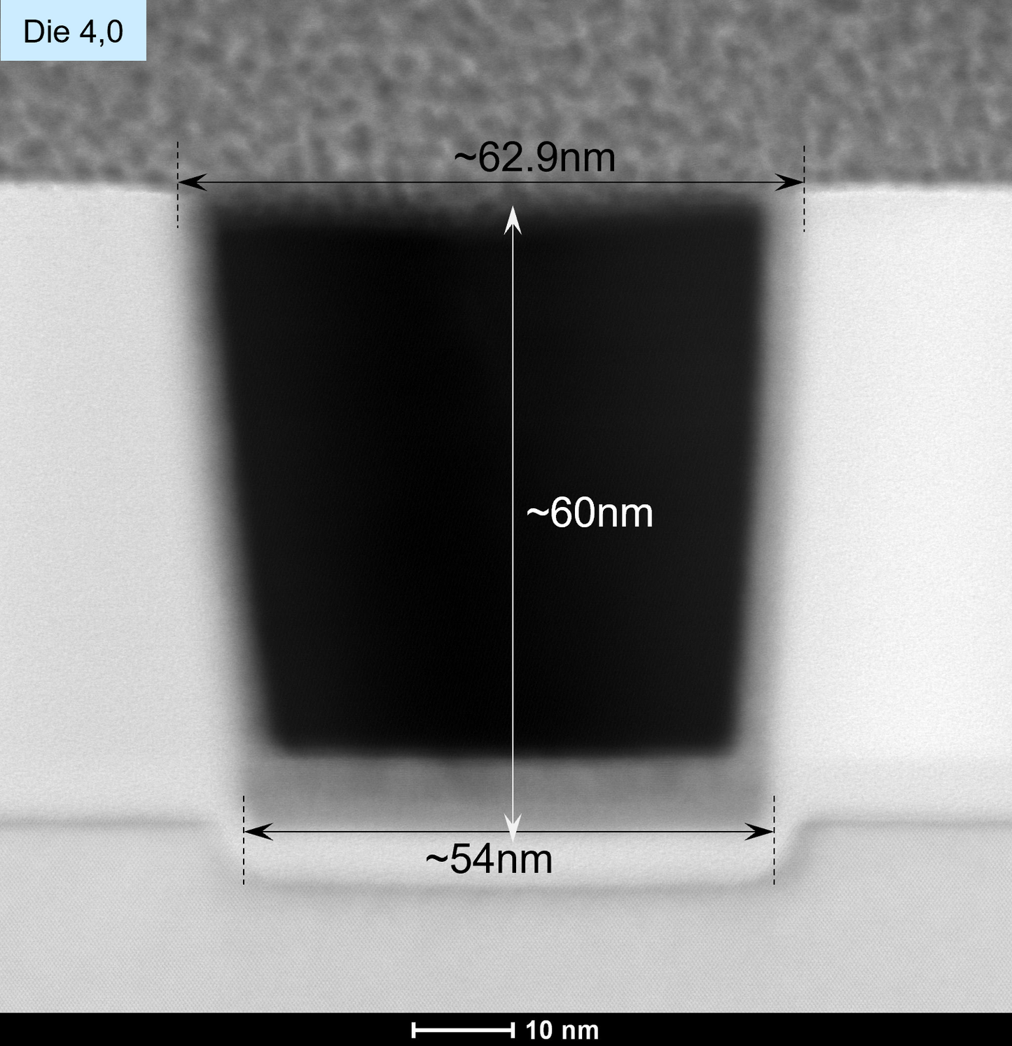
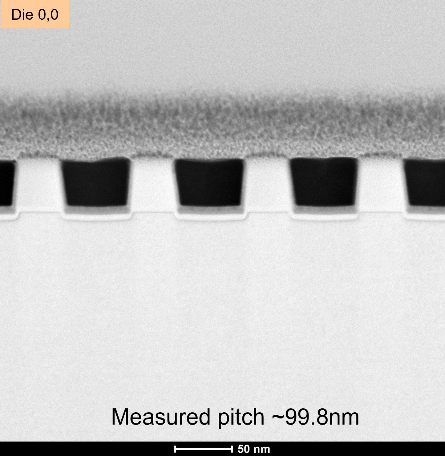
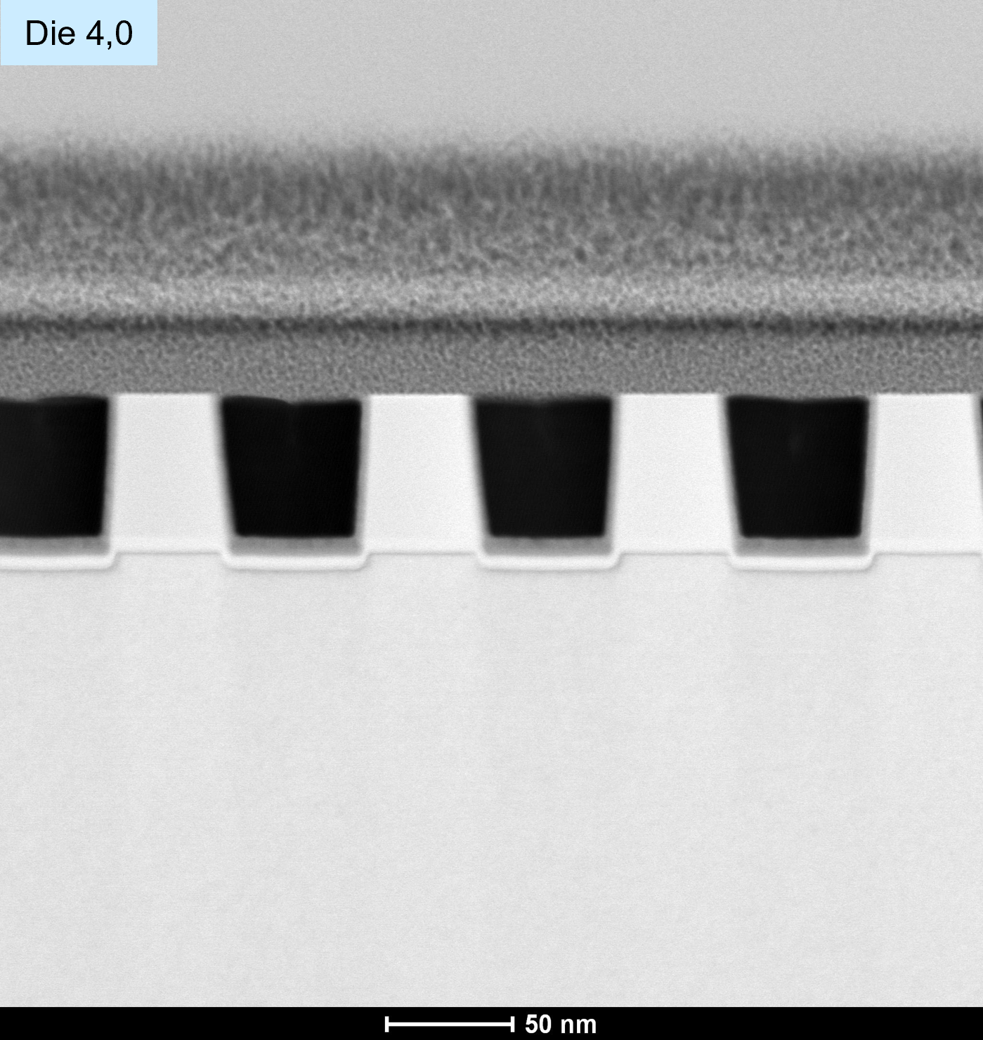
- Stack: AMAG's Cu/W CMP wafers use our existing AMAG7 Hardmask LineSpace wafer stack (etched oxide line/space on Si substrate with 100nm oxide height), coated with adhesion film then Cu or W dep, and then CMP down to where metal ~50 nm thick on L50P100 anchor target.
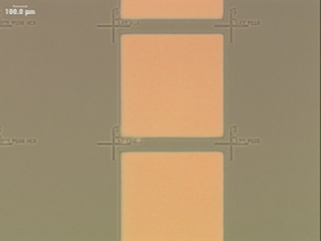
- Density gradients and AMAG7: AMAG7 was designed to give a platform for lots of roles all built into one reticle. The entire grating array is one big across-field density DOE. The field includes 547 large pad-size gratings (0.8 mm pad with 0.1 mm moat) spanning CD/pitch/form factor. AMAG7 is designed to be one big CMP experiment, with each grating big enough for uniform un-dished pattern in middle, but dishing will vary condition-to-condition around grating edges. Our strategy is to optimize to anchor target at L50P100 and the rest will perform relative to the optimum. That feature should be best and other patterns should degrade as pitch is increased away from 100 nm, and density thus changes across the field and around various gratings.
| Wafer | 300 mm standard, 200 mm option available |
| Process | AMAG7, L50P100 LineSpace, ~100 nm depth |
| Stack | 100 nm SiO2 on Si, lines etched in SiO2, terminate on Si substrate; Tungsten level: 30A RF Ti+30A ALD TiN + 4kA CVD W CMP |
| Depth | ~60 nm post CMP |
| Pattern | AMAG7, Full Field, 27 mm x 33 mm, 59 die |
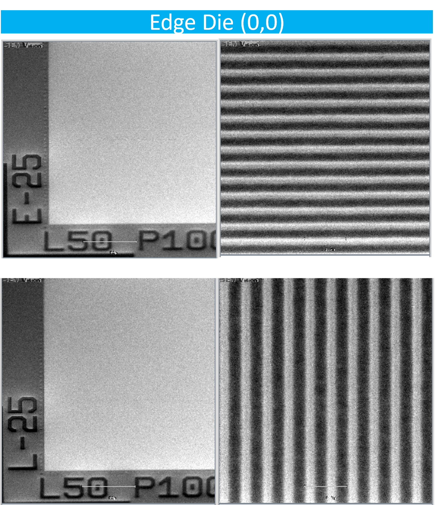
| Anchor target | L50P100 downsized to L47P100 |
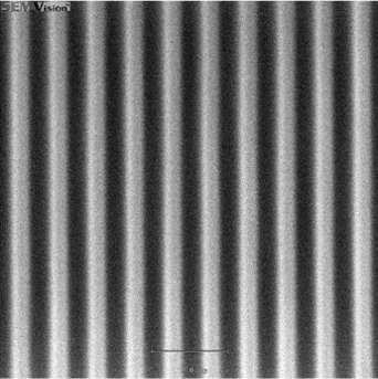
| Imaged targets | L50P100, L55P110, L60P120, C120 Faux Memory |
| CD, Anchor Target | Bottom CD: ~50 nm |
| Reference metrology |
Anchor target: CD measurements & images,all sites/wafer. Reports: "100nm depth oxide HM (L50P100) Line & Space, navigation & results": "100nm depth oxide HM (L50P100) Line & Space with 30A ALD TiN Coating, navigation & results": |
Regular price
Regular price
Sale price
Unit price
per
Couldn't load pickup availability
